- IC 555 TIMER Pin Configuration
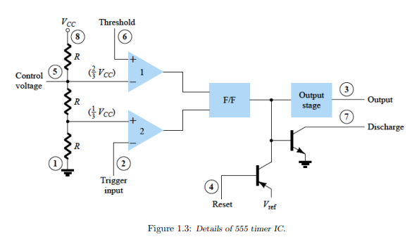
The pin configuration is represented in figure 1.2. This IC consists of 23 transistors, 2 diodes and 16 resistors. The use of each pin in the IC is explained below. The pin numbers used below refers to the 8-pin DIP and 8-pin metal can packages. The circuit diagram of IC555 timer is shown in figure 1.3. These pins are explained in detail below:
Pin 1: Grounded Terminal: All the voltages are measured with respect to the Ground terminal.
Pin 2: Trigger Terminal: The trigger pin is used to feed the trigger input hen the 555 IC is set up as a 1-1 1-2 Lecture 1: IC555 Timer Figure 1.2: 555 Timer IC Pin Configuration monostable multivibrator. This pin is an inverting input of a comparator and is responsible for the transition of flip-flop from set to reset. The output of the timer depends on the amplitude of the external trigger pulse applied to this pin. A negative pulse with a dc level greater than Vcc/3 is applied to this terminal. In the negative edge, as the trigger passes through Vcc/3, the output of the lower comparator becomes high and the complimentary of Q becomes zero. Thus the 555 IC output gets a high voltage, and thus a quasi stable state.
Pin 3: Output Terminal: Output of the timer is available at this pin. There are two ways in which a load can be connected to the output terminal. One way is to connect between output pin (pin 3) and ground pin (pin 1) or between pin 3 and supply pin (pin 8). The load connected between output and ground supply pin is called the normally on load and that connected between output and ground pin is called the normally off load.
Pin 4: Reset Terminal: Whenever the timer IC is to be reset or disabled, a negative pulse is applied to pin 4, and thus is named as reset terminal. The output is reset irrespective of the input condition. When this pin is not to be used for reset purpose, it should be connected to + VCC to avoid any possibility of false triggering.
Pin 5: Control Voltage Terminal: The threshold and trigger levels are controlled using this pin. The pulse width of the output waveform is determined by connecting a POT or bringing in an external voltage to this pin. The external voltage applied to this pin can also be used to modulate the output waveform. Thus, the amount of voltage applied in this terminal will decide when the comparator is to be switched, and thus changes the pulse width of the output. When this pin is not used, it should be bypassed to ground through a 0.01 micro Farad to avoid any noise problem.
Pin 6: Threshold Terminal: This is the non-inverting input terminal of comparator 1, which compares the voltage applied to the terminal with a reference voltage of 2/3 VCC. The amplitude of voltage applied to this terminal is responsible for the set state of flip-flop. When the voltage applied in this terminal is greater than 2/3Vcc, the upper comparator switches to +Vsat and the output gets reset.
Pin 7 : Discharge Terminal: This pin is connected internally to the collector of transistor and mostly a capacitor is connected between this terminal and ground. It is called discharge terminal because when transistor saturates, capacitor discharges through the transistor. When the transistor is cut-off, the capacitor charges at a rate determined by the external resistor and capacitor.
Pin 8: Supply Terminal: A supply voltage of + 5 V to + 18 V is applied to this terminal with respect to ground (pin 1).
Comments
Post a Comment