Posts

Image
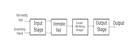
  An operational amplifier is a direct-coupled high gain amplifier usually consisting of one or more differential amplifiers and usually followed by a level translator and an output stage. The output stage is generally a push-pull or push-pull complimentary symmetry pair. An operational amplifier(op-amp) is available as a single integrated circuit package. Input Stage  − The input stage is the dual input, balanced output differential amplifier. This stage provides most of the voltage gain and introduces the input resistance of operational amplifier. Intermediate Stage  − This stage is dual input, unbalanced output differential amplifier, which is driven by the output of first stage. Level Shifting Stage  − Since direct coupling is used, therefore the DC voltage at the output of intermediate stage is above the ground potential. Hence, the level shifting transistor circuit is used after intermediate stage to shift the DC level at intermediate stage output downward to zero volts with resp
Image
                                                    IC 555 TIMER   Pin Configuration  The pin configuration is represented in figure 1.2. This IC consists of 23 transistors, 2 diodes and 16 resistors. The use of each pin in the IC is explained below. The pin numbers used below refers to the 8-pin DIP and 8-pin metal can packages. The circuit diagram of IC555 timer is shown in figure 1.3. These pins are explained in detail below:  Pin 1: Grounded Terminal: All the voltages are measured with respect to the Ground terminal.  Pin 2: Trigger Terminal: The trigger pin is used to feed the trigger input hen the 555 IC is set up as a 1-1 1-2 Lecture 1: IC555 Timer Figure 1.2: 555 Timer IC Pin Configuration monostable multivibrator. This pin is an inverting input of a comparator and is responsible for the transition of flip-flop from set to reset. The output of the timer depends on the amplitude of the external trigger pulse applied to this pin. A negative pulse with a dc level greater than Vcc/